Built for semiconductors.
We learn how your chip teams really work, from the first block to sign-off, and put AI to work in the tools they already use.
Request a briefingFloorplans, timing and verification, learned from the engineers who close your designs.
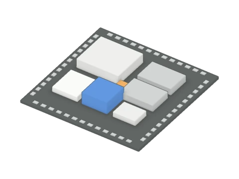 Floorplanning
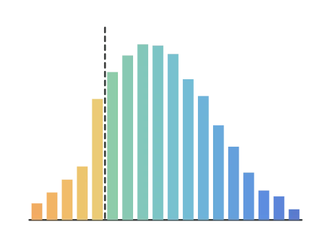 Timing closure
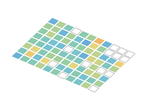 Verification coverage
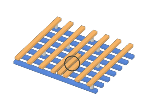 Layout checks
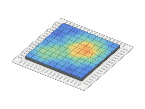 Power analysis
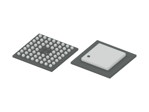 Package design
Yield, recipes and tool data, learned from your process and equipment engineers.
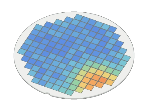 Wafer maps
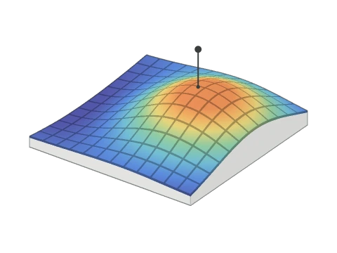 Recipe tuning
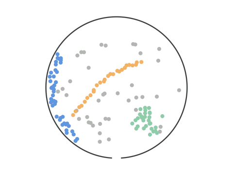 Defect classification
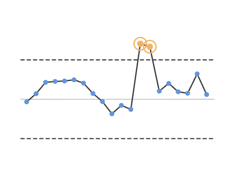 Process control
 Tool maintenance
 Shift handover
Who it is for
- Chip Design
- Design and verification teams working towards a tape-out.
- Equipment
- Engineers who build and service the tools a fab runs on.
- Fabs
- Process and yield engineers keeping a line in spec.
Where the work happens
- Implementation
- Synthesis, place and route and timing closure in Synopsys and Cadence tools.
- Verification
- Simulation and formal runs, and the debugging when one of them fails.
- Sign-off
- Timing and physical checks, down to the last clean report in Siemens Calibre.
- Process and yield
- Recipes, excursions and yield reviews, where one lot can decide a quarter.
What good work means
A chip team is judged on a tape-out that works the first time.
A respin costs months and a new mask set. Timing, power and area decide what counts as done, so that is what the work is measured against.
Your data stays yours
Design files are the company. They stay inside it.
Each person owns the record of their own work and decides what the team sees. We never measure individual productivity. Security, privacy, legal and the works council are at the table from the first week.
How we start
One team, one workflow, one baseline.
A sponsor picks a team of five to ten people and one workflow. We sit with them for four weeks, then review the result together against the measure agreed at the start.